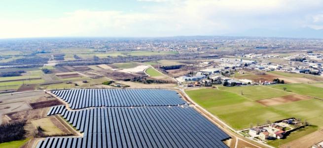
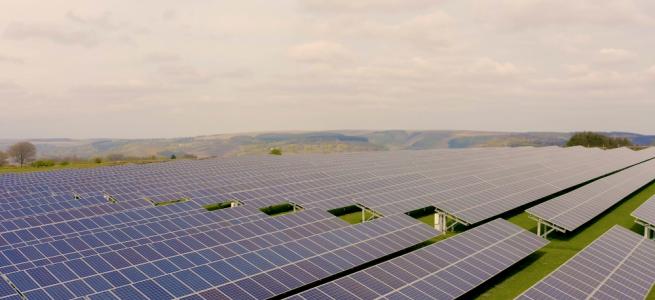
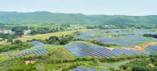
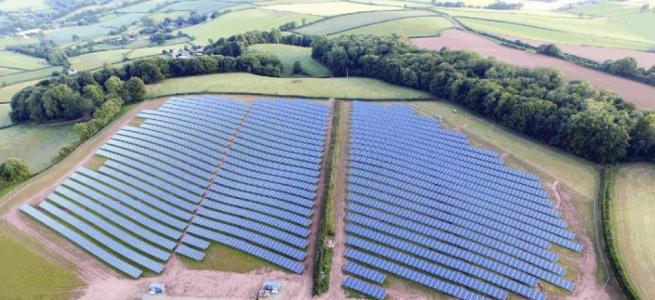
FEATURE: Working the advantage of thin film
 Thin film photovoltaics using perovskites as a light absorbing material are a very recent development and they could propel the third generation of photovoltaics by a colossal step. The scientists at the Belgian research institute imec in Leuven have been vigorously focusing on this subject for some time Philip Pieters, the director in charge of business development at imec explains the advantages of this thin film photovoltaic technology and points out potential applications.
In the realm of thin-film technologies imec is currently focusing on the development of solar cells with perovskites as the light absorbing material. Why of all things have you adopted this specific technology?
In the past we had done many developments in the realm of organic photovoltaics. At the same time several firms emerged, first Konarka, and later Heliatek, Beletric OPV, Armor and Eight 19. In organic photovoltaics we managed to reach efficiencies of 12 to 12.5 percent. That was quite good. But then we noticed the ongoing developments based on perovskites. At first we were somewhat hesitant to enter this field, because it looked pretty much like hype. But then we investigated this technology closer because we recognized that it is a technology with great potential.
.
How far have you gotten up to now?
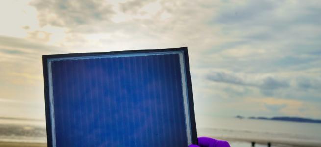
When we started developing solar cells based on perovskites we quickly achieved efficiencies of 15 percent. This was possible because we could draw on our rich experience in organic photovoltaics. In the mean time, we are getting as much as 18.5 percent efficiency with small cells having a size of 20 square centimeters. This is of course not the world record, which today stands at 21 percent and higher. But our focus is less on creating cells with ever higher record numbers, which exhibit their record marks only on small surface areas. Instead, we feel obliged to prove that we can reach this efficiency in large areas as well. Therefore, we concentrate on increasing the cell and module sizes and on transferring the technology to the realm of industrial manufacturing.
How are you tackling this task?
On the basis on our perovskite cells, which have an efficiency of 18 percent, we are enlarging the surface area in which the light absorbing material is deposited. At a module size of 150 to 160 square centimeters we can still achieve an efficiency of 11 to 12 percent. Yet at larger sizes the efficiency goes down. The task here is to maintain the current efficiency value even across large surfaces. In the end we want to realize complete cells measuring 156 by 156 centimeters with this material and achieve up to 20 percent efficiency.
What printing processes are you using for this?
Initially the objective is to realize the cells on a rigid carrier material. As a substrate glass is best suited, but metal sheets could also be used. We are doing this on our production line in Leuven. There we deposit the different materials in single quantities on glass substrates using the slot-die coating process. But from the end of the year on we also want to adopt the roll to roll process and thus print the materials on flexible substrates. This will be done in the facilities of our R&D partners at Solliance in Eindhoven. At Solliance there is a lot of experience in roll to roll printing technology. This development, which we be kicked-off in the coming year, because the roll to roll process has the advantage of higher throughput.
Now, what are the challenges of printing perovskites?
They are similar to those in organic photovoltaics: The layers must be printed and deposited at the highest possible uniformity. Since we have developed the process already for OPVs we can now control this quite well. Here too we can benefit from our experience with OPVs, since these basically use very similar manufacturing processes, and the production machinery is almost identical as well.
What efficiencies are you striving for in the framework of upscaling the process?
Evidently the efficiency should be as high as possible. So far, we have achieved 12 percent on 150 to 160 square centimeters. I think we must now drive this up to 20 percent and higher for this cell size, and then transfer this value to large surfaces. We see yet another application of perovskites "“ by combining them with crystalline silicon cells and this way achieve efficiencies of 28 to 30 percent for the entire tandem pack.
What would such a combination look like?
We will put the perovskite semiconductor on top of the silicon cell. Then the crucial factor determining the efficiency will be the interconnect type. There are two options to do this. You can interconnect the tandem cell as one complete stack, with one contact on top of the perovskite layer and another contact beneath the silicon cell. This will be simpler to manufacture. But the problem here is that you must ensure current matching across the entire stack. With this variant, the effective efficiency is limited, since the two cells are affecting each other. Therefore, the second option, a fourfold contacting scheme, is better suited in regard to the total efficiency of the tandem cell. This way, each part of the stack is contacted separately, and each part of the tandem cell operates under its own optimum condition, without being impacted by the others. However, this is certainly more demanding when implemented in a mass production environment, but is justified by its higher energy yield. In this scheme you can interconnect the silicon cell entirely in the back by utilizing, for instance, the IBC technology, which is readily available.
How will this impact the energy generation?
We have simulated this with various light spectra. Separately interconnecting the individual parts of a stack achieves a significant increase in yield. After all, the light spectrum is not constant over the course of the day. It is different in the morning, midday and evening. If the individual cells are affecting each other they cannot realize their respective advantages for a certain light spectrum.
Do you have the same possibilities with perovskites cells as organic photovoltaics offers it, in regard to design variations?
At the moment we are looking primarily at opaque perovskite cells. But we have already demonstrated that semi-transparent cells and modules based on perovskites are feasible as well. This is of particular interest for building integration, where the task is to integrate semi-transparent perovskite films in windows. This will be necessary in the future to fulfill the higher energetic demands on buildings. Semi-transparent perovskite films will be of special importance in high-rise buildings since their roof surfaces will not be large enough. Different colors are possible as well. These we will achieve by band gap variations.
When will we see the first perovskite modules coming to market?
Dyesol is in the process of establishing the appropriate manufacturing facilities. I think the company will bring out their first products in the not so far future. To reach properly up scaled production lines will take some time still. But it will be faster than in the realm of OPV since the fundamentals are already in place.