Laser processes for increasing solar cell and module efficiency
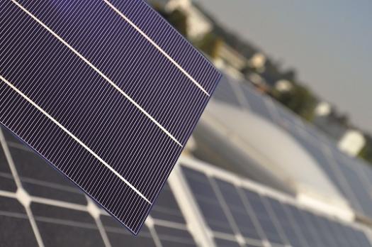
Laser processing of crystalline solar cells
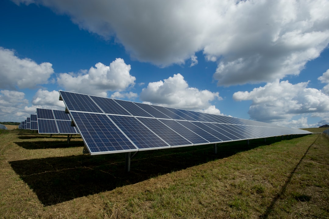
One approach to increasing PV cell effectiveness with moderate additional plant investment is the so-called PERC concept (passivated emitter rear cell) made of crystalline silicon that utilises improved backside surface passivation to increase efficiency. This is realized by the application and processing of bulk layers of aluminum oxide (AlOx) and silicon nitride (SiN). Laser technologies can play an important role to further reduce costs during PV cell and module production. Examples include precise laser reopening of backside layers in PERC cells as well as cleaving solar cells into half cells to improve current yield. Lasers can also play a role by replacing other soldering processes in cell-module connections.
PERC technologies as the starting point
PERC technology has entered mass production; early adopters can be found in Taiwan and across the global marketplace. PERC cell efficiency of 21 percent and more has been well demonstrated by a number of manufacturers. The essential advantage of PERC technology is the comparatively simple integration of the additional required process steps into existing production lines without costly, large-scale plant upgrades. Existing technology can be used along with PERC-specific steps and previous productivity optimizations can be retained. PERC investments in modern production technology amortizes quickly for manufacturers. Figure 1 shows the basic structure of a PERC solar cell schematically. The main advantage is the supplementation of electrical surface passivation through the cells' back-sides using aluminum oxide and silicon nitride. Typical layer thicknesses for AlOx can range up to 30nm while the thickness of SiN layers can range from 80-100nm. Si wafer surfaces can be both textured and polished. During the course of the subsequent production process, these dielectric passivation layers must be partly reopened without damage to the underlying silicon in order to ensure contact between the exposed metal layer and the silicon.

Fig. 1: Schematic depiction of the stack layout of PERC solar cell (source: ISFH)
Using laser ablation to open the insulating layer
Laser technology is suited for microstructuring crystalline solar cells. It enables a high throughput and very good economy; it can be reliably integrated into production lines. Its key advantages compared to masking or electron beam processes are economy and superior throughput. Additional advantages are non-contact energy coupling, flexible beam guidance, high accuracy, and rapid positioning as well as exact control of energy infeed. Material damage is avoided; breakage rates are minimized.
When fabricating PERC cells, a main focus is on selective, non-destructive removal of the AlOx and SiOx or SiN passivation layers (Fig. 1) implemented by either a dot or line pattern. If utilising the dot pattern approach individual dot sizes range from 80μm-150μm, while the separation distance between individual dots is typically 0.4mm-1 mm depending upon customer requirements.
Using the line pattern approach, widths are typically 30μm-120μm and line separation distance should be between 0.7 mm and 1.5 mm for most applications.
The wafer"˜s backside is contacted using screen printing after successful structuring. Different laser sources ranging from nanosecond lasers to ultra-short pulse lasers can be utilized in PERC cell manufacturing depending upon the customers' quality, throughput, and investment thresholds. A galvo scanner with a working area greater than 160 x 160 mm² is used for processing wafers with a size of 156mm x 156mm. Nanosecond lasers score points mainly in terms of throughput and cost efficiency. However, the pulse duration does have a thermal influence on the material being lasered. Processing with both 532nm and with infrared (1064nm) ultimately prove successful. In an industrial setting, infrared lasers with high repetition rates are generally preferred since they hold clear advantages in terms of acquisition and maintenance costs as well as power utilization and service life. Processing speeds of up to 15,000 mm/s are achieved with it (Fig. 2).

Depending upon material properties a thermal influence from laser-induced heating is detectable. This is an important consideration because excessive energy input can lead to melting and damage to the crystal structure, which in turn can influence local dosing ratios. Varying levels of thermal influence can lead to increased recombination of charge carriers and thus to a performance degradation in the solar cells. The potential for damage and reduced performance must be carefully evaluated by the manufacturer so that optimal opening behaviour can be achieved in the crystal structure without reducing the benefits of rear side passivation. PV cell manufacturers should depend upon laser technologists with years of experience, process understanding, and the ability to conduct process development in close co-operation between both parties to realize desired efficiency gains. Laser ablation with ultra-short pulse durations in the pico and femtosecond range (10-13 s to 10-15 s) offers advantages. These lie in the laser's ability to impart all of its energy to the material within a very short time interval. Extremely high power densities up to a few gigawatts per cm² are thereby achieved. This leads to very good absorption of the laser radiation and the associated possibility of processing quasi-"athermal" results with extreme precision.
Ultra-short pulse duration can impart qualitatively high-value structures with practically no negative heat influence or contamination of the surrounding material. Ultra-short pulse lasers can be integrated as reliably into fabrication processes as nanosecond lasers; however, they are clearly more cost intensive both to acquire and to maintain. Ultra-short pulse lasers deliver results that are virtually flawless (visually) as evidenced in Figure 3. The laser also delivers passivation layer processing with extraordinary selectivity; a heat-affected zone is nearly unrecognisable.
In contrast to the nanosecond laser, it was also possible to realize processing with significantly less power. These extraordinarily promising results hold out hope for rapidly reducing operational costs by using ultra-short pulse laser sources along with typical PERC cell processing equipment elsewhere along the production line.
From a technical perspective, PV cell production laser equipment is needed that brings about precise surface structuring with minimal crystal damage. From a commercial perspective this optimized processing technology needs to also lower operating costs as a market-entry criterion for PERC technology [2]. Laser source selection currently complies in essential ways with the throughput, geometry, and the stoichiometric framework conditions of the layer to be structured. A robust machine concept is needed that meets the cell manufacturer"˜s specific requirements.
Among these today is realizing throughputs of more than 3,600 wafers per hour. This throughput will need to double within ten years to meet demands projected in the ITRPV roadmap. In addition to high throughput, breakage rates of less than 0.1 per cent must be ensured. Moreover, short maintenance and service cycles as well as high machine availabilities of >95 percent need to apply in standard production.
To achieve high-throughput, low breakage and virtually continuous availability, innovative cell handling concepts with effective cost-benefit ratios are needed.
These benefits can be achieved with laser processing on-the-fly (OTF). OTF processing has the advantage of eliminating costly handling and individual positioning of PV cells within the machine. Instead, the wafers are transported on a conveyor belt under the laser source, which renders stops for orientation superfluous. An integrated lens automatically compensates for relative cell motion during structuring of the passivation layer by the laser. The conveyor belt"˜s continuous clocking leads to a nearly 100 percent utilization of the laser source. The implementation of "˜non-touch' cell handling can enable an additional production optimization.
This handling concept is based upon a technology that avoids mechanical contact between the wafers. Gentler, more frictionless wafer transport within the plant is thereby guaranteed during the laser process. Cell breakage or micro cracks (cell damage that can later lead to breakage) are avoided, thus realizing a higher yield. This smoother handling also paves the way for the further reduction of wafer thickness in further cell technologies. Further advantages of non-touch handling result from the system"˜s minimal maintenance cost as well as lower power consumption in comparison to conventional start/stop transport systems.

Half-cell cutting to increase PV module power with TLS-Dicing
Discussing PV cell manufacturing yield, throughout and unit cell performance enhancements would not be complete without considering half-cell concepts. A technologically promising path towards higher module efficiencies without increasing cell efficiencies themselves is central to the concept of a half-cell module [3], [4]. Major benefits supporting the half-cell concept include reduced series resistance loss combined with better light management that occurs when more sunlight reflected from the back-sheet reaches active cell areas [5], [6]. This can lead to an increase in module efficiency of about 3 percent (relative). However, care is needed throughout the cell separation process because it might induce electrical or mechanical damages to the cells, which either lower the electrical performance of the module or could cause reliability issues. The standard industrial process of p-type cells is based on a laser scribing on the cell rear side (30-100 μm deep,) and subsequent mechanical cleaving. The disadvantages of mechanical cleaving can include reductions in cell efficiency, reduced mechanical strength and substantially greater handling costs due to the combination of a laser process with subsequent cleaving steps. An alternative process is cell separation based on Thermal Laser Separation (TLS-Dicing/TLS). TLS is used in the semiconductor industry's back-end to separate semiconductor wafers into components. The process is based upon thermal induced m generated by a well-adjusted combination of a laser heating and cooling. Thus, a crack is guided through the entire cell and two half-cells are obtained.
The method is suitable for most brittle materials in the semiconductor industry, including Si, SiC, Ge and GaAs wafers. [7]. Compared to traditional separation technologies, TLS is virtually damage-free; it offers impressive clean, micro-crack-free edges and greater resulting bending strength.
The complete cleaving is a one pass process with a speed of up to 300 mm/s. The relatively low temperature (no material is ablated or melted) in combination with the high cleaving speed are the reason that the electrical properties are not influenced by the separation step. Furthermore, the high throughput and wear-free processing offer great potential for reducing production costs and cost of ownership. It has been demonstrated that cells separated using the TLS process show a significantly higher mechanical strength, better edge quality as well as a lower power reduction compared to laser scribing and cleaving approaches. [8].
First-class laser system yield and efficiency
3D-Micromac AG has taken the demonstrated potential of the most advanced laser technologies into account and further developed existing production systems for photovoltaics in order to meet cell manufacturers"˜ demands. The microSTRUCT OTF, a highly reliable production tool, was developed and successfully introduced to the market for laser backside opening. The system is characterized by a compact structural form, an innovative handling concept and minimal infrastructure requirements.
The mature machine platform is suitable both for new production lines and for equipping existing lines. The modular structure can be combined with any number of laser sources to match the system exactly to respective process requirements. The complete system encompasses the laser processing station and handling. Throughput amounts to more than 3,600 wafers per hour depending on the contact openings"˜ structuring geometry. The suitability for industrial cell production has been successfully demonstrated and confirmed by customers. 3D-Micromac has adapted its advanced laser technology for cutting solar cells into half cells. The resulting system, the microDICE OTF, also achieves a throughput of 3,600 cells per hour by using on-the-fly technology. It guarantees the highest productivity and an outstanding price-performance ratio. The microDICE OTF is a fully automatic 24/7 production solution and can be offered as a stand-alone or inline system.
All 3D-Micromac production solutions are designed to meet cell manufacturers' demands for achieving maximum throughput rates and yield while cutting cell processing costs. The systems guarantee very high availability through the use of sophisticated concepts and high quality / high efficiency components.