Technical Insight
Solar cells: Taking efficiency to new highs
An inverted metamorphic architecture offers a route to making lightweight, incredibly efficient, cost-competitive cells for space.
BY PAUL SHARPS, DANIEL DERKACS AND ALEX HAAS FROM SOLAERO TECHNOLOGIES


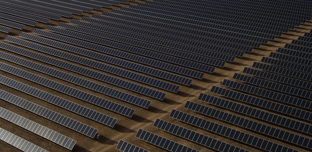
Although III-V multi-junction cells have been deployed on earth to generate electricity, they are delivering their greatest commercial success in space. Out there they are highly valued for their high efficiency and robustness, particularly to particle radiation. What's more, they offer tremendous economic value at the system level by reducing satellite launch and operating costs. Together, these attributes make III-V cells ideal for supporting satellite missions requiring either a high specific power (W/kg) or a high power density (W/m2).
At SolAero Technologies of Albuquerque, NM "“ which took over Emcore's solar business in late 2014, while retaining all its expertise and capability "“ we have a great track record in improving the efficiency of our III-V multi-junction cells. Between 1998 and 2008 the measured efficiency of multi-junction cells under conditions replicating those in space increased from 23 percent to 29.5 percent (for these measurements, radiation was incident under no concentration (1 sun) with a spectrum mimicking that of the sun's before it passes through the earth's atmosphere (AM0)).
These efficiency figures might suggest that our focus is on the production of a handful of cells with incredibly high efficiencies. But that is certainly not the case: we pride ourselves on the production of vast numbers of highly efficient cells. Over the past 18 years we have manufactured more than 3 million large-area space cells, defined as having an area of at least 26 cm2. The knowledge gained from this has helped us to produce cells that have an initial efficiency of 29.5 percent and deliver 85 percent of this value at the end of a 15-year geosynchronous mission. Even now, we are not resting on our laurels, but pursuing a roadmap that involves the development of far more efficient devices that incorporate metamorphic structures and more absorbing layers.
Solar designs
Manufacture of our solar cells is based on multi-junction designs, rather than single-junction variants, because this leads to better spectral utilization and reduced thermalization losses. Multi-terminal and mechanically stacked architectures are options for the fabrication of these multi-junction devices, but we prefer two terminal devices, because this trims costs associated with cell fabrication and system integration.
In a two-terminal device, the cells are connected by lattice-matched Zener tunnel diodes, which reverse the polarity between each of the subcells. This allows multiple n-on-p subcells to be monolithically stacked on top of each other. The voltage produced by the multi-junction device is equal to the sum of those produced by each subcell, and optimisation requires the design of each n-on-p junction to produce the highest voltage possible without reducing the photo-generated current.
During the last two decades, the primary source of satellite power has been the triple-junction device formed from lattice-matched layers of GaInP, InGaAs and germanium (see Figure 1). The foundation for this is a p-type germanium substrate, on which GaInP and InGaAs layers are grown by MOCVD. During growth, the group V element from the nucleation layer diffuses into p-type germanium, converting a thin layer on the surface to n-type. This creates a diffused n-on-p junction. To provide precise lattice matching to the germanium substrate, a small amount of indium is added to the middle InGaAs junction.
SolAero's Satellite Flight Heritage
With this device, the internal quantum efficiency of all sub-cells approaches 100 percent (see Figure 2). Consequently, there is little room left for improvement in the current collection in this device.
Where gains can be made is in photocurrent. In these monolithic, two-terminal multi-junction cells the subcells are connected in series, so the same current must flow through all of them. This means that it is possible for one or more subcell to fail to operate at its maximum power point. For example, in a device with a GaInP/InGaAs/germanium architecture and bandgaps of 1.88 eV/1.40eV/0.67 eV, the germanium subcell is capable of generating twice as much current as it does in this triple-junction stack (see Figure 3). Due to this, the multi-junction cell will deliver an inferior performance to that of a cell with all junctions operating at individual maximum power points.
Improvements could result from increasing the bandgap of the bottom junction so that it adds to the operating voltage while still generating enough current to avoid limiting the overall device. Alternatively, gains could be made by lowering the bandgap of the top two subcells to increase cell efficiency through superior spectral utilization and improved current matching at each subcell's maximum power point.
With either of these approaches, or by adding to the number of junctions, it is possible to improve upon the AM0 efficiency limit of approximately 30 percent for the GaInP/InGaAs/germanium device. It is worth noting, however, that the obvious approach of adding more junctions suffers from a law of diminishing returns. So, assuming that the cost of every added subcell is the same, there is a point at which the increased efficiency comes at a price that the market will not bear.
Attempts to increase solar efficiency tend to involve either employing mechanical stacks, turning to novel materials, or creating metamorphic structures. Here we will we briefly describe the first two, before discussing in more detail the third option, which is the one that we pursue. Note that there are many III-V semiconductor materials that can be combined into multi-junction devices (see Figure 4), and we limit ourselves to monolithic devices, because, as previously stated, this trims cell fabrication and integration costs.
Pros and cons of stacking"¦
Mechanical stacking of cells to improve performance has made the headlines, because this class of device holds the efficiency record for devices operating under concentrated illumination (sunlight is focused by a factor of several hundred on to the cell). The great attraction of mechanical stacking is that it removes the bandgap/lattice constant constraint, opening the door to designs that combine a wide range of bandgaps with different lattice constants.
One example of a mechanically stacked cell is the pairing of a GaInP/GaAs dual junction grown on a GaAs substrate with a GaInAsP/GaInAs dual junction grown on InP. The resulting device, with bandgaps of 1.89 eV, 1.41 eV, 1.00 eV, and 0.73 eV, is close to ideal for the maximum conversion efficiency for the space spectrum.
This device is created by wafer bonding, a process that forms a mechanically robust, optically transparent, electrically conductive interface between the component multi-junction cells. The challenge is cost. This approach requires a separate growth for each of the component multi-junctions, one of which involves a very expensive InP substrate.
Costs could fall by turning to epitaxial lift-off, but this technology is still to be demonstrated to the degree required to significantly lower the substrate growth costs. Another drawback is that to ensure that the surfaces are adequately flat for wafer bonding, they must be polished with a chemical-mechanical process. If particles or growth imperfections are present, they prevent wafer bonding in local areas. Due to all these issues, despite its high efficiencies, mechanical stacking is simply too expensive to be considered for space applications.
Figure 1. The GaInP/InGaAs/germanium lattice-matched, triple-junction cell is monolithic device that is grown on a germanium substrate.
Figure 2. The internal quantum efficiency (IQE) of the Zener tunnel-junction cell overlaid on the space AM0 spectrum.
"¦ and novel materials
Novel materials are attractive, because they provide the opportunity to replace the germanium subcell with one of a higher bandgap, or to insert a 1.00 eV subcell between the germanium and InGaAs subcells to create a four-junction device. With the latter approach, a 1.0 eV subcell is grown directly on the germanium substrate prior to the growth of GaInP and InGaAs subcells.
The two most popular candidates for a 1 eV cell are the dilute nitride InGaAsN(Sb) and the ternary SiGeSn. Both materials have the virtues of an independent lattice constant and bandgap (within ranges). This allows a tuning of bandgap while retaining lattice matching to GaAs or germanium.
A four-junction cell based on InGaP, GaAs, InGaAsN and germanium was first proposed in 1997 by a group at Sandia National Labs in Albuquerque, NM. However, due to the poor material quality of the MOCVD-grown InGaAsN junction, this cell never realised its expected performance. In addition, the device was expensive to grow. Progress has been made since then, by growing the InGaAsNSb layers by MBE, and incorporating them into triple-junction GaInP/GaAs/InGaAsNSb cells. These devices have produced an efficiency in excess of 30 percent under 1 sun, AM0 conditions, but the MBE growth process is expensive, partly because of the low throughput.
Development of the alternative, SiGeSn, is still in its infancy. Junctions made from this ternary are yet to produce voltages consistent with their bandgap. Another concern is that this material is meta-stable, and requires a growth temperature of less than 400°C. Further fundamental studies are needed before this ternary can be incorporated in a multi-junction device.
Mighty metamorphics
We advocate a metamorphic approach, which includes upright and inverted structures. If upright metamorphic multi-junction structures are produced, the lowest bandgap subcell should be grown first, followed by higher bandgap subcells (see Figure 5(a)). With this architecture, the bottom junction is typically made from germanium, and above this are the metamorphic grading layers and finally the metamorphic subcells.
For this class of metamorphic cell, which tends to feature GaInAs-based metamorphic subcells, compositions of the III-Vs follow the GaAs-InAs tie line. The indium content is gradually added to the step grades to reach the appropriate lattice constant.
A major downside of this approach is that all of the epitaxial layers are lattice mismatched with respect to the substrate, and consequently contain threading dislocations. This is a major drawback, because the threading dislocations act as carrier recombination sites that degrade solar cell performance through increased dark current and reduced photo-generated carrier collection. Since all of the epitaxial layers are metamorphic in these upright multi-junction structures, all tend to suffer from non-optimal performance for the particular bandgap.
Figure 3. Individual and aggregate current-voltage curves for the GaInP/InGaAs/germanium solar cell. The germanium junction operates at the current-matched point in the complete triple-junction device, rather than at its maximum power point.
Figure 4: Bandgap and lattice constant for a number of semiconductor materials, with the III-V materials of particular interest for multi-junction cells noted.
Defects are minimised, and cell performance optimized, by using the other class of metamorphic "“ the inverted metamorphic multi-junction. In this case, devices are grown "˜upside down'. This means that the high bandgap junctions are grown first, lattice matched to the substrate, followed by lower bandgap metamorphic "˜boost' junctions.
An example of this "“ a triple-junction inverted metamorphic "“ is shown in Figure 5(b). It features two lattice-matched subcells and one metamorphic subcell. The initial high bandgap subcells, such as GaInP, GaAs, InGaAlP and AlInGaAs, are grown lattice matched to the germanium growth substrate, and they generate the majority of the power from the cell. The metamorphic subcells, meanwhile, produce a smaller proportion of the generated power than they would in an upright metamorphic multi-junction structure.
To produce this class of cell we attach the structure to a "˜processing handle', such as silicon or kapton, before removing the growth substrate. Epitaxial layers are between 10 μm and 15 μm thick, depending on the number of subcells in the device, and the processing handle can be temporary, necessary only for processing; or it can be permanent, providing an integral part of the final device.
Figure 5: (a) The upright metamorphic four-junction cell has a performance that is compromised by threading dislocations through the entire structure. With inverted metamorphic cells with three (b) or six (c) junctions, only part of the structure suffers from threading dislocations.
Figure 6: Internal quantum efficiency and reflectance for the inverted metamorphic, six-junction cell.
There is great freedom with this approach as devices can be flexible or rigid, and structures can be packaged for the end application. Selection of an appropriate permanent handle enables a very light cell, and ultimately a very high specific power (W/kg). This approach is ideal for epitaxial lift-off, where the epitaxial layers are removed from the substrate along a laterally etched release layer.
We have demonstrated inverted metamorphic cells with three, four and even six junctions (see Figure 5(c) for a representation of a six-junction cell, and Figure 6 for internal quantum efficiency and reflectance measurements from an actual six-junction cell). Using such a high number of junctions is cost competitive with current, commercially available space multi-junction cells, because production employs existing MOCVD growth technology and known fabrication practices.
Table 1. Comparison between modelled space inverted metamorphic cell (black) performance and NASA verified (red) performance, for the 1 sun, AM0 spectrum.
We have also undertaken a comparison between modelled and verified efficiencies (see Table 1, where the numbers in red are the NASA verified measurements, and the black numbers are the results of our model). Note that the performance modelling is based on a "˜practical' approach that considers the likes of optical reflectance and series resistance. Based on these findings, we have a path for increasing efficiency beyond 30 percent to nearly 38 percent. Given this promise, the inverted metamorphic cell is expected to be the core technology in the next generation of commercially available cells for space applications.