Slashing the cost of the GaAs solar cell

Sol Voltaics aerosol growth process promises to kick-start a market for terrestrial solar cells based on GaAs. Richard Stevenson interviews CEO Erik Smith
Q:Your company is developing GaAs nanowire solar cells that are produced with an aerosol-based growth technology. Do you see the primary market for your technology as a low-cost solution to increasing the performance of silicon solar cells, via the creation of tandem cells? Or is your technology going to be used for the manufacture of standalone nanowire cells?
A:The end product of our technology is basically a solar film. It can be used standalone, terrestrial, or it can be used in tandem cells.Typically, penetrating the household rooftop [market] is the beginning for new materials, because you don't have as many bankability issues. When it's rooftop you can still go single-junction, which is just standalone, or tandem, depending on what your output needs to be. The single-junction will be extremely cost-per-Watt competitive. Tandem is upper 20 percent efficiencies, at costs equivalent to silicon. So it depends what your goal is.
Q:What's the attraction of a III-V-and-silicon cell in the terrestrial market? Why not just deploy silicon cells?
A: III-Vs have always been considered one of the highest efficiency cells on the market in a single junction. III-Vs also benefit significantly from what [cadmium telluride solar cell manufacturer] First Solar benefits from, which is a very good temperature coefficient. So in very hot climates the cells don't degrade nearly as much as silico n.
Q:Back in 2016, at the CS International Conference, speaker Frank Dimroth from the Fraunhofer Institute for Solar Energy Systems included in his talk an evaluation of the market opportunity for III-V-on-silicon cells. He presented calculations based on the MOCVD growth of a five micron-thick III-V film, and concluded that costs would need to fall by two orders of magnitude before this technology could make an impact. Do you agree with this view that if III-Vs are to have a place in the terrestrial solar cell market, the technologies that are to be used need to be many tens of times lower in cost than they would be with traditional technique s?
A:There's no way that you can grow an MOCVD-based film and have a tandem that is cost effective. It's not going to work. I can't comment on tens or twenties, or multiple orders of magnitude, because I don't know what I'm orders of magnitude against. But all I know it has to be cost effective. We have done bottom-up cost models, and we're going to be extremely effective.I also know that other III-V companies have, for example, been bought by Chinese companies. They are not cost-effective. That's the reason they were bought for pennies on the dollar.
Q:Is the business plan to license the process and sell aerosol-based growth reactors?
A:Our business plan can go in a number of ways, and I'm not going to comment, but all of those that you can imagine are viable. They all have pros and cons.
Q:What is the essence of your growth technology?
A:It's extremely similar to MOCVD growth methodology "“ but without the wafers, which are expensive, and without the high costs of MOCVD.
Q:Why are production costs lower than they are for the likes of MBE and MOCVD, growth technologies that are suitable for high-volume manufacturing?
A:It's a combination of the fact that we can rain nanowires in a continuous process, that the nanowires grow at one thousand times the rate that they grow in an MOCVD tool, and the fact that we use 80 percent less material than wafer based solar cells, because of the photonic effects. [Note that] we make a solar film "“ it is not wafer based.
Q:How do you ensure homogeneity when growing the nanowires?
A:Well, it's a single crystal, and it's the same growth mechanism as MOCVD. Growth starts from a seed. Once we produce those nanowires, they come out like a dust. You have mis-orientated nanowires, and you have to align them. We do that beautifully, with over 99 percent alignment and orientation.This ability to make nanowires and control their alignment, whether they are gallium arsenide, gallium arsenide phosphide or amorphous silicon nanowires, could be more than solar.
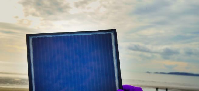
SolVoltaics' process produces a film of doped, aligned gallium arsenide nanowires. Once passivated, they can form a film with an efficiency of more than 15 percent.
Q:You passivate the nanowires. Have you optimised this process?
A:Yes, passivating the nanowires is critical to making a good solar cell. You could have a solar cell in gallium arsenide that is not passivated, but it's a pretty poor solar cell. The fact that we have demonstrated a 15.3 percent nanowire solar cell is indicative of good passivation.
Q:What are the optimal dimensions for your nanowires?
A:Typically, diameters are somewhere between 150 and 200 nanometres, and the length of the nanowires between two and three microns.
Q:What is your current record for nanowire efficiency, and how high an efficiency is possible?
A:Our record is 15.3 percent. The roadmap for efficiency from that point on is very clear on what needs to be changed. How to change those things and how to improve those things is also clear. For example, optimising the emitter length, the TCO, and the contact etch. Within the gallium arsenide community it is known how to improve all those things. Right now, 24 percent is the clear, visible roadmap. And Alta Devices has had cells at 28, 29 percent.
Q:Are your aerosol-based reactors now ready for solar cell manufacture?
A: Actually, we have not announced some things so I don't want to say too much, but we have two different aerosol reactors up and running right now. One is more advanced than the other. They are producing wires.
Q:With your reactors, how long can they run for before they require any maintenance?
A:That's the whole optimisation that we are going through as a company right now. When our newest tool came up, it was running at a certain number of hours a day, and now it's running at a much better number of hours per day.We have basically done the R&D, and now it's about optimising everything. So to optimise the equipment you change an injection flow, you change a material here, and you change an exhaust type there "“ you do all of these things to start optimising the equipment.
Q:One of the substantial costs associated with epitaxy is the capital cost of the growth reactor. How does this compare to the cost of building your tools?
A:I'm familiar with MOCVD tools and CVD tools. If you look at the cost of the tool, there's lots of steal, there lots of pneumatic panels, there are lots of pumps and gases used. All I can say with respect to cost is the cost of the tool itself is not the significant part. It's still mostly the materials and the integration of the cells. The fact that it's a non vacuum, continuous process [with our approach] enables us to be lower in cost than a standard batch semiconductor process.
Q:What are the waste products in your process, and how do you treat them?
A:Everything is recycled. Every solar manufacturer has to have a methodology to recycle the modules after their lifetime. We have programs ongoing now that will meet that criteria when the product comes to end of life. We have to do all that stuff. There are waste gases in the process, because you are not utilising all your materials. And those are also recycled.
Q:You have raised tens of millions of dollars in funding. How far can this take you?
A:Starting from 2011, we have raised $58 million, but that also includes a lot of non-diluted funding. About 25 percent of that is non-diluted, so non-equity type money. It is from the EU, or from the Swedish Energy, or from the other Scandinavian programmes. If we were in Silicon Valley, it would have cost a lot more to get where we are today. We would have needed almost double that what we need here.
Q:What do you need to do before you start generating sales?
A:It depends somewhat on where you initially go with generating sales. If you go after the utility sector, then that takes longer. The spectrum for solar is anywhere from little dinky consumables to utility and space stuff. But samples for customers are going to be coming out in 2018, and then it depends on the business model. The preliminary business model may be a little different than the mid-range business model, versus the long-range business model. Our business model, it might be where our customers decide to take it.
Sol Voltaics' GaAs nanowire film could be used to boost the efficiency of silicon and CdTe solar cell via the formation of a tandem architecture.


