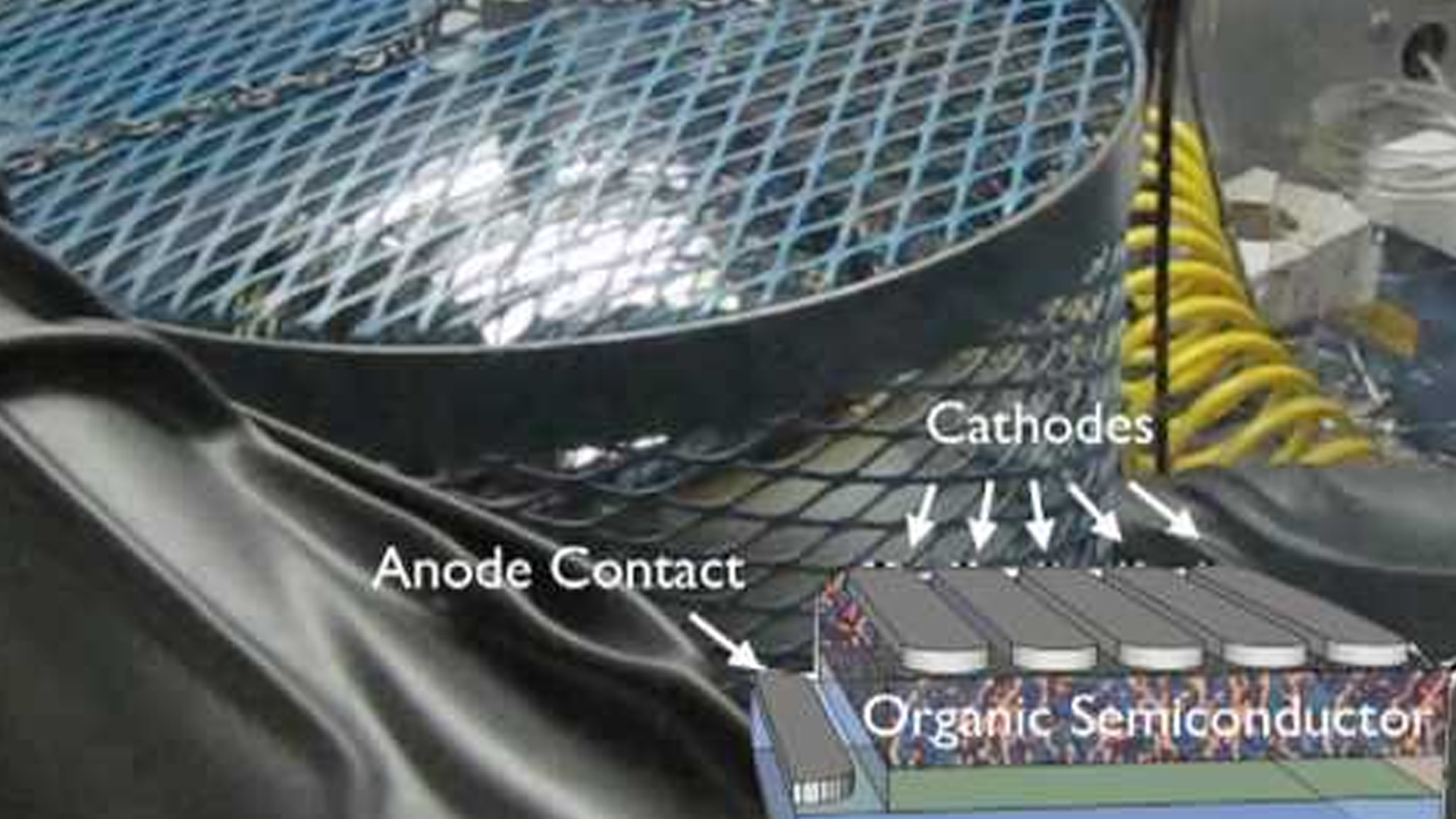
See Through Solar

If solar cells were transparent they could be fitted to windows and building
facades. Physical modeling helps in the development of
suitable materials for transparent electronics and thus in creating the basis
for transparent solar cells.
Offering
a view of the garden and an adjacent field, it looks like any other window. But
this window offers an additional feature: it also produces electricity. The
facades of the house, too, harness solar energy to supply the occupants with
electrical power. This is what the domestic power supply of the future could
look like. The surface area used to produce energy would increase greatly with
transparent solar cells.
To
translate the vision of see-through solar cells and transparent electronics into
reality, two different transparent coatings would be required - one to conduct
the electricity via electrons, the n-conductors, and one in which electron holes
enable the electricity to flow, the p-conductors. To produce these coatings the
engineers dope the base material with a few other atoms. Depending on which
atoms they use, they obtain the differently conducting coatings. N-conducting
transparent materials are state of the art, but the p-conductors are
problematic. Their conductivity is too low and often their transparency is poor.
Manufacturers need a transparent base material which is amenable to both n- and
p-doping.
At
present, indium tin oxide is mainly used for the n-conductors, but this is
costly. Indium has become a rare commodity and its price has increased tenfold
since 2002. The search for substitute materials is therefore in full swing. At
the same time, various questions need to be answered, such as which materials
would be best suitable, what they should be doped with to obtain good
conductivity, and how good their transparency is. Research scientists at the
Fraunhofer Institute for Mechanics of Materials IWM working in cooperation with
other Fraunhofer colleagues have developed material physics models and methods
which help in the search. “If transparent p-conductors with adequate
conductivity could be produced, it would be possible to realize completely
transparent electronics,” says Dr. Wolfgang
Körner,
research scientist at the IWM.
Using
electron microscope images, the researchers initially determine the grain
boundaries which most frequently occur
in the material - i.e. irregularities in the ordered crystal structure. These
defect structures are modeled atom by atom. Special
simulation methods calculate how the electrons are distributed in the structures
and thus in the solid body. From the data the researchers extract how conductive
and transparent the material is. “We have found, for example, that phosphorus is
suitable for p-doping zinc oxide, but that nitrogen is more promising,” says
Körner.