NTNU-researchers reveal tuning a small strain on single nanowires
NTNU researchers Dheeraj Dasa and Helge Weman have, in cooperation with IBM, discovered that gallium arsenide can be tuned with a small strain to function efficiently as a single light-emitting diode or a photodetector. This is facilitated by the special hexagonal crystal structure, referred to as wurtzite, which the NTNU researchers have succeeded in growing in the MBE lab at NTNU. The results were published in Nature Communications this week.
The last few years have seen significant breakthroughs in nanowire and graphene research at NTNU. In 2010, Professors Helge Weman, Bjørn-Ove Fimland and Ton van Helvoort and their academic group went public with their first groundbreaking discoveries within the field.
The researchers, who specialise on growing nanowires, had succeeded in controlling a change in the crystal structure during nanowire growth. By altering the crystal structure in a substance, i.e. changing the positions of the atoms, the substance can gain entirely new properties. The NTNU researchers discovered how to alter the crystal structure in nanowires made of gallium arsenide and other semiconductors.
With that, the foundation was laid for more efficient solar cells and LEDs.
"Our discovery was that we could manipulate the structure, atom by atom, said Helge Weman from the Department of Electronics and Telecommunications. "We were able to manipulate the atoms and alter the crystal structure during the growth of the nanowires. This opened up for vast new possibilities.
We were among the first in the world who were able to create a new gallium arsenide material with a different crystal structure."
The process exists in nature as in diamond and graphite, the latter is used as the "lead" in pencils, are composed by the same carbon atoms but their crystal structures are different.
The next discovery was made in 2012. At that point, the researchers had managed to make semiconductor nanowires grow on graphene. This discovery was described as a revolution in solar cell and LED component development.
Over time, graphene can replace silicon as a component in electronic circuits. Today, silicon is used for producing both electronics and solar cells. Graphene conducts electricity 100 times faster than silicon, and is only one atom thick, while a silicon wafer is normally millions of times thicker. Graphene will also likely be cheaper than silicon in just a few years.
The research group received a lot of international attention for the graphene method. Helge Weman and his NTNU co-founders Bjørn-Ove Fimland and Dong-Chul Kim were encouraged to establish the company CrayoNano AS, working with a patented invention that grows semiconductor nanowires on graphene. The method used is molecular beam epitaxy (MBE), and the hybrid material has good electric and optical properties.
" We are showing how to use graphene to make much more effective and flexible electronic products, initially solar cells and white light-emitting diodes (LED)," says Weman. "The future holds more advanced applications such as highly effective solar cells."
"Our goal is to create solar cells that are more effective than when they are made with thin film technology," Weman emphasises.
Thin film technology is a term from the solar cell technology. This technology develops super-thin solar cell panels, where the active layer converting sunlight to electricity has a thickness of no more than three micrometres, i.e. three thousands of a millimetre. The low weight allows easy transportation, installation and maintenance of the solar cells, and they can in practice be rolled out like roofing felt on most buildings.
The combination of nanowires and graphene facilitates much broader and more flexible solar cells. In thin films like gallium arsenide, the atoms are placed cubically in a fixed, predefined structure. When the researchers manipulate the atom structure inside the nanowire, they can grow both cubic and hexagonal crystal structures. The different structures have completely different properties, for example when it comes to optical properties.
The last couple of years the research group has, among other things, studied the unique hexagonal crystal structure in the GaAs nanowires.
" In cooperation with IBM, we have now discovered that if we stretch these nanowires, they function quite well as light-emitting diodes," explained Weman. "If we press the nanowires, they work quite well as photodetectors.
This is facilitated by the hexagonal crystal structure, called wurtzite. It makes it easier for us to change the structure to optimise the optical effect for different applications."
" It also gives us a much better understanding, allowing us to design the nanowires with a built-in compressive stress, for example to make them more effective in a solar cell. This can for instance be used to develop different pressure sensors, or to harvest electric energy when the nanowires are bent."
Because of this new ability to manipulate the nanowires' crystal structure, it is possible to create highly effective solar cells that produce a higher electric power. Also, the fact that CrayoNano now can grow nanowires on super-light, strong and flexible graphene, allows production of very flexible and lightweight solar cells.
The CrayoNano group will now also start growing gallium nitride nanowires for use in white light-emitting diodes.
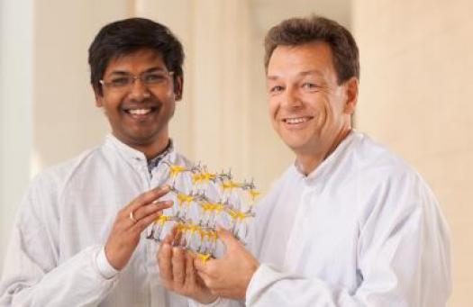
IMAGE: Dr. Dheeraj Dasa and Prof. Helge Weman at Norwegian University of Science and Technology.
Credit: Photo: Kai T. Dragland/NTNU