Seamless integration of thin-film photovoltaics in the built environment

Over the last decade the industry has witnessed the growth of crystalline Si based photovoltaics at the expense of thin-film technologies. This has led many to rethink the opportunities offered by thin-film photovoltaics and the technological needs to serve specific markets like building-integrated photovoltaics where thin-film photovoltaics would offer unique opportunities. What are the requirements to integrate photovoltaics in the built environment and what are the consequences this vision has on research and development strategy in the field of thin-film photovoltaics? Tom Aernouts - Group leader organic photovoltaics Jef Poortmans - Scientific Director Photovoltaics, Professor at K.U.Leuven from imec discuss.
Energy Efficiency is a keyword in many strategic documents about the evolution towards a sustainable energy system (IEA, EU Commission, "¦). Given the fact that the energy used in buildings accounts for a significant part of the energy consumed (20-40 percent ), it is clear that improving energy efficiency in buildings will be a crucial factor towards the goal of a more sustainable energy system. This is the rationale behind European directives (see e.g. EU directive 2010/31 on energy performance of buildings and its translation in national legislation). In these directives it is stated that Member States shall ensure that by 31 December 2020, all new buildings are nearly zero- energy buildings and after 31 December 2018, new buildings occupied and owned by public authorities are nearly zero-energy buildings. This has to be achieved by measures at or near the building.
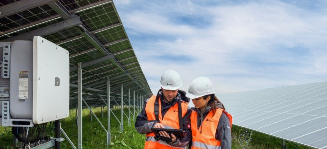
It is obvious that the integration in buildings represents a unique opportunity for PV-modules at the condition they are integrated in an aesthetically attractive way in the building and can serve multiple purposes besides generating electricity like protection against external moisture, partial shading to reduce cooling requirements in the building, ventilation, "¦ Especially the aspect of aesthetics is not be underestimated. In this context building-integrated photovoltaics (BIPV) is to be discriminated from building-added photovoltaics (BAPV). In the latter the PV-modules are just added on an existing building, whereas in the former the integration of the PV-module in the building envelope of the new or to be renovated building is part of the design process from the beginning which results in aesthetically much more appealing solutions. It is also becoming more and more clear that in order to reach this improved aesthetics, architects and project developers would like to go beyond the use of standard PV-modules in terms of dimensions, shape, outlook, colours and transparency as to leave them a maximum of free design space. These aesthetical aspects combined with the multi-functionality of the PV-module "“ it is to be considered as a building component rather than a pure electricity generating device "“ are also an attractive opportunity for the PV-industry as it opens up the possibility of broadening product competition scope beyond the level of pure costs on the level of Euro/Wp.The knowledge about the local rules and norms for buildings and the close interaction with building component companies is a necessity to be successful in this emerging market. This represents obviously an excellent opportunity for a value chain in which European-based companies can build up a sustainable business model.
Building-integrated photovoltaics and thin-film photovoltaics
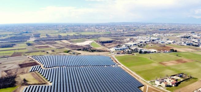
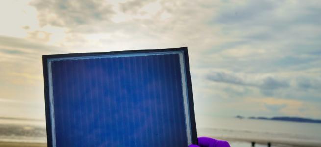
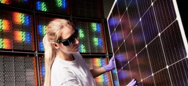
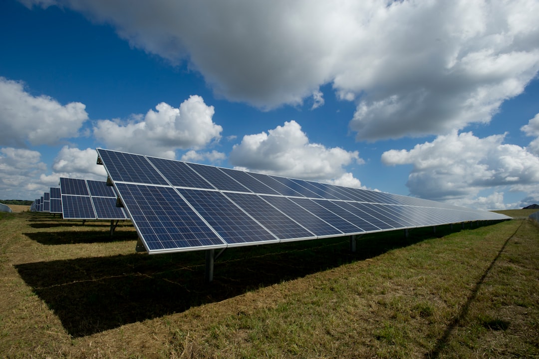
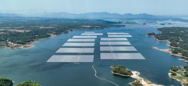
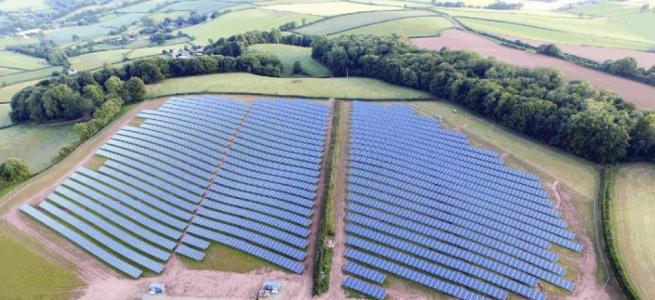
Thin-film photovoltaics has a number of assets which make it particularly attractive to reach the improved aesthetics and design freedom requirements outlined above. The rather naïve idea over the last decades that thin-film PV would replace crystalline Si based PV purely based on cost advantages has to make way for a more realistic view that thin-film PV will in first instance make it in applications where some of its unique properties can be exploited to the full extent. BIPV is definitely such an area. The possibility to integrate thin-film PV on a broad variety of carriers, either flexible or rigid, its homogeneous outlook extending to the possibility of reaching for homogeneous semi-transparency, its response under indirect light and its reduced T-coefficient are all important assets which are less easily achieved by crystalline Si. These assets have been proven in a number of attractive demonstration projects.
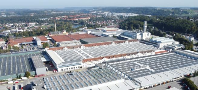
Fig. 1 Artist impression of building integrated PV

Maximum design freedom with thin-film PV freeform module technology
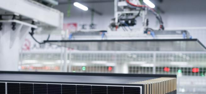
Beyond these favourable features of thin-film PV for BIPV, the design freedom for the architects, project developers and the design of the electrical system of the building can be further enlarged by developing a thin-film PV module technology which deviates considerably from the industrial practice nowadays. The present practice for thin-film PV module technology is still mostly based on the traditional sequence of layer deposition followed by a scribe to define the separate cells and realize the interconnection between the cells. This procedure has been optimized for different thin-film PV technologies in terms of reduced dead area etc. but leaves relatively room for varying dimensions and also reduces the freedom on parameters like output voltage of the module (the voltage is essentially determined by the number of cells in series which is fixed). To cope with these limitations came the idea to disruptive module technology development where first all the layers are being deposited on a substrate and only afterwards the scribes are made and the interconnections are being realized by printing. This leads to an interesting restructuring of the value chain in the sense that the front-end of the process (deposition of all the layers, e.g. by a glass manufacturer which would like to increase the value of its end product) is now separated from the back-end part of the process (the scribing and printing) which can now be executed by the building component manufacturer or a company working closely together with the latter. Such a freeform module technology development will be specific for different active absorber materials as it relies on depth selectivity of the different scribes and the realization of contacts with low contact resistance and stable contact interfaces.
Freeform module technology development in imec and Solliance
Within the Solliance consortium, in collaboration with Smit Ovens, novel equipment has already been developed, addressing this back-end technology. It allows for inline laser scribing of thin-film PV modules whereby the interconnects are finalised with an additional inkjet printed line of Ag-based conductive ink. The Solliance consortium has the ambition to demonstrate this newly developed process flow on two main thin-film PV technologies, being the more established CIGS technology, and the newly emerging Perovskite based thin-film PV technology.
In the current thin-film PV market, mainly three different technologies are commercially available. Where over 10 years ago amorphous-Si was by far the largest market for thin-film PV (above 10% of the total PV market), nowadays it has been shrinking to below 1 percent of the total PV market. Nonetheless, the excellent progress in performance, both in efficiency and reliability, that has been achieved in the last few years for thin-film PV technologies like CdTe and CI(G)S, in combination with cost-competitive production has ensured that thin-film PV was able to maintain its market share in an overall growing PV market still at the level of 7-9 percent. Noticeable there is also that CIGS is substantially growing its share, reaching a 1.5 GW production in 2014, whereas CdTe is stagnating and a-Si even declining. It is believed that CIGS will indeed continue this growth and so becoming the lead TF-PV technology for the coming years.
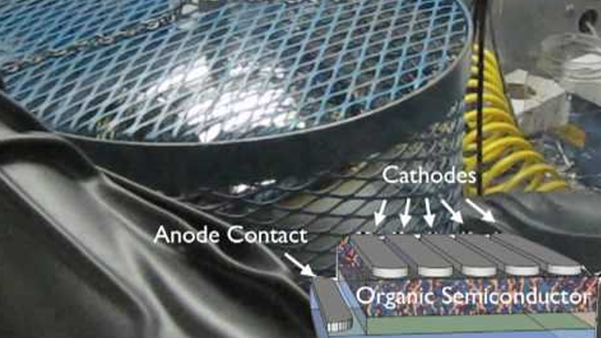
The emergence of organic-inorganic Perovskite materials in the field of photovoltaics occurred actually by introducing these compounds as potential dye material in dye-sensitized solar cells. Rapidly it turned out that the Perovskite material has also very good charge transporting properties making first the use of an electrolyte and later even the mesoporous TiOx-structure obsolete. This resulted in a device architecture whereby a single, planar layer of Perovskite material of ~300nm, sandwiched in between selective contact layers, acts as an efficient absorber, charge generation and charge transporting medium. This development took less than 5 years to raise the efficiency from the level of a few percent to a current state-of-the-art 20.1%.
Since this performance has not yet been demonstrated neither for pure organic nor for dye-sensitized solar cells, perovskite-based photovoltaics has raised a lot of attention and is considered nowadays as the highest potential next generation thin-film PV technology. Nonetheless, two major concerns are to be taken into account, next to developing scale-up of this technology, before perovskite PV can be actually brought into market applications. The first one is the issue with stability, whereas current understanding is that control of humidity is crucial to enable device operation lifespans of many years. Secondly, the current perovskite compounds used for PV contain a central lead atom. For health, safety and environmental reasons alternatives have to be found to replace this component.
The Solliance consortium has a strong track record in CIGS device and process developments and will complement that further with demonstration of this new back-end process still this year. The developments in the field of Perovskite modules are based on the strong background that Solliance has built up already in the field of organic photovoltaics.
Conclusion
Thin-film PV modules have unique characteristics (can be integrated on a broad variety of substrates, can be made semitransparent with a homogeneous outlook, have a good response under indirect light, ...) that make them the ideal candidates for realizing multifunctional electricity-generating building components. But for architects and project developers to be able to use these building components, more flexibility needs to be introduced. A thin-film technology is required that allows to adjust dimensions, shape, outlook, color, transparency and even output voltage of the PV module.
Within the framework of the Solliance consortium, a new thin-film PV module technology is being developed that fulfills this need. It is a freeform module technology in which first all layers are deposited on a substrate and afterwards the scribes are made and interconnections are printed. This new technology makes it possible to restructure the value chain: the building material supplier (e.g. glass manufacturer) deposits all the thin-film PV layers on the material and the building component manufacturer uses this material to finalize the product (e.g. a solar window) by scribing and printing the contacts. This latter party can determine dimensions, shape, outlook etc. It is our conviction that such a new technology and business model will enable to accelerate the development and market introduction of building-integrated PV.