European Partnership For Next Generation Of Stacked Solar Cells
Thin-film solar modules are an inexpensive and versatile
alternative to traditional solar cells made of crystalline silicon. Eighteen
leading industrial and research partners have joined forces in an EU Fast Track
project aiming to further refine this technology. In the next three years, it
is planned to produce a marketable prototype with an efficiency of twelve
percent. The project is coordinated by Forschungszentrum Juelich and funded to
the tune of € 9.3 million by the EU.
In recent years, various companies have increased the
efficiency of marketable thin-film solar modules to the present level of ten
percent. Although these modules are still not as efficient as conventional
solar cells, they can be produced much more economically. In the case of
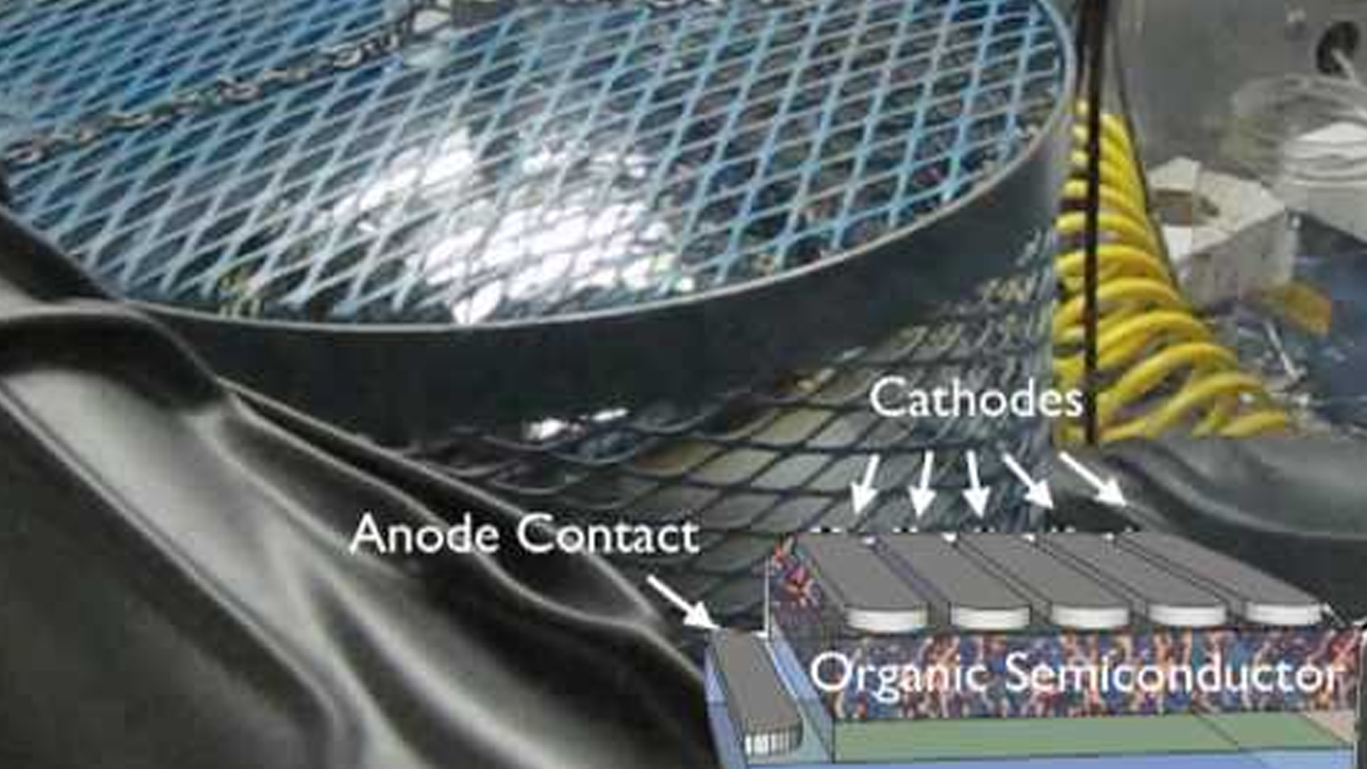
thin-film modules, the silicon is applied to the substrate in a layer about one
micrometre thick and does not need to be carefully cut out from expensive
wafers. Thin-film silicon solar modules designed as tandem solar cells are
particularly efficient. They consist of two layers one on top of the other,
which absorb different fractions of sunlight.
Each of these two cell layers is divided into several
sublayers which all influence each other in a complex manner. Since these
interactions are difficult to predict, existing industrial thin-film solar
cells make use of proven combinations of components and substrates. In the Fast
Track project, leading representatives from research and industry who previously
pursued different technologies are now pooling their expertise in order to
combine the best components. By harmonizing and optimizing different
approaches, a new generation of thin-film silicon solar modules will be created
with an efficiency of twelve percent. This corresponds to an increase of twenty
percent and under test conditions the costs should amount to less than € 0.5
per watt nominal power
In order to achieve this goal, the researchers will
experiment with various nanomaterials and optical functional layers and refine
the entire process chain. "The basic difficulty consists in adjusting the
different components to each other. A slight modification that improves the
conductivity of one of the upper layers may, for example, have a negative
impact on the current densities generated in the lower layers," explains
project coordinator, Dr. Aad Gordijn from Forschungszentrum Juelich. The
scientists in the Fast Track project aim to influence the optical and
electronic properties even more effectively by making use of nanocrystalline
silicon dioxide "“ a novel "multiphase" material, whose solid structure displays
greater degrees of freedom than pure silicon.
The surface condition of the various layers is also being
scrutinized. Structures on a nanometre scale will help to improve light
trapping. However, it is not yet possible to predict what the perfect
light-scattering layer will look like.
"We are going to test superimpositions
of different structures based on craters or pyramids in order to arrive at an
optimized morphology," says Gordijn.
The project was launched on 1 March 2012
and will run until 28 February 2015. Then, at the latest, a new prototype
should be available as a model for industrial production.