New Stanford manufacturing process could yield better solar cells, faster chips
Computer chips, solar cells and other electronic devices have traditionally been based on silicon, the most famous of the semiconductors, that special class of materials whose unique electronic properties can be manipulated to turn electricity on and off the way faucets control the flow of water.
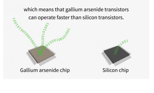
There are other semiconductors. Gallium arsenide is one such material and it has certain technical advantages over silicon "“ electrons race through its crystalline structure faster than they can move through silicon.

But silicon has a crushing commercial advantage. It is roughly a thousand times cheaper to make. As a result, gallium arsenide-based devices are only used in niche applications where their special capabilities justify their higher cost.
Cellphones, for instance, typically rely on speedy gallium arsenide chips to process the high-frequency radio signals that arrive faster than silicon can handle.
Now Stanford researchers have invented a manufacturing process that could dramatically reduce the cost of making gallium arsenide electronic devices and thus open up new uses for them, notably inside solar panels.
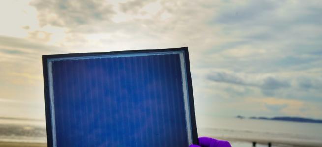
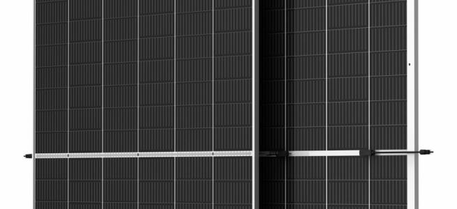
"Solar cells that use gallium arsenide hold the record when it comes to the efficiency at which they convert sunlight into electricity," said Bruce Clemens, the professor of materials science and engineering who led this work.
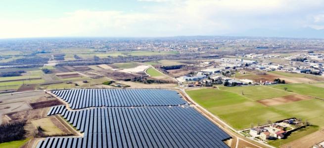
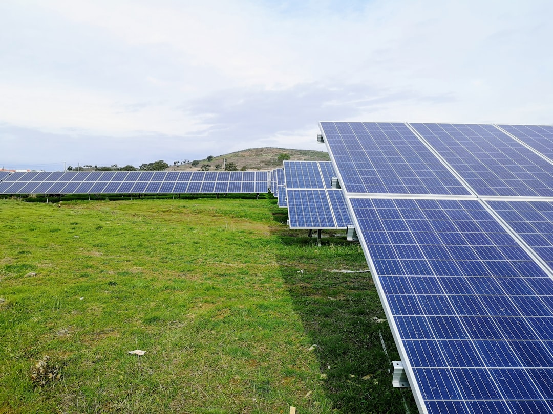
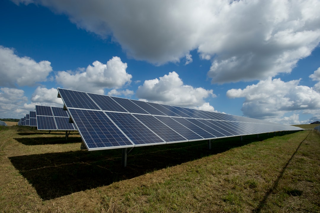
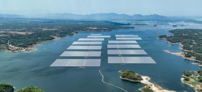
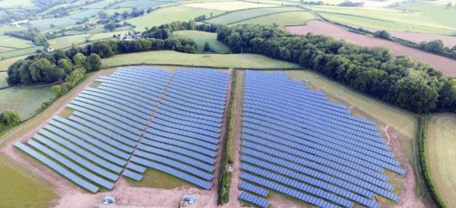
But silicon-based solar is so much cheaper to make that gallium arsenide solar cells are relegated to exotic applications such as satellites. There, the main cost is launching the satellite into orbit, so gallium arsenide solar panels pay their freight by virtue of their greater photon-to-electricity conversion efficiency.
Clemens, who is the Walter B. Reinhold Professor in the School of Engineering, said the Stanford process could make gallium arsenide solar cells more practical on Earth.
Writing in the journal MRS Communications, Clemens and co-author Garrett Hayes, who recently earned his doctorate in materials science from Stanford, describe this new manufacturing process.
Silicon and gallium arsenide both begin their progression from raw crystal to electronic device similarly. Both materials are fashioned into what electronics manufacturers call wafers. These are flat, circular platters of purified material. Subsequent manufacturing steps create computer chips, solar cells or other electronic devices on top of these wafers.
But it can cost about $5,000 to make a wafer of gallium arsenide 8 inches in diameter, versus $5 for a silicon wafer, according to Aneesh Nainani, who teaches semiconductor manufacturing at Stanford.
The new Stanford process seeks to lessen this thousand-to-one cost differential by reusing that $5,000 wafer.
Today the working electronic circuits in a gallium arsenide device are grown on top of this wafer. Manufacturers make this circuitry layer by flowing gaseous gallium arsenide and other materials across the wafer surface. This material condenses into thin layer of circuitry atop the wafer. In this scenario, the wafer is only a backing. The thin layer of circuitry on top of this costly platter contains all of the electronics.
To make the wafer reusable the Stanford process would add several steps to the manufacturing process. The researchers demonstrated the technique in their experiments.
First they covered the precious wafer with a layer of disposable material.
Then they used standard processes of gas deposition to form a gallium arsenide circuit layer on top of the disposable layer.
Next, using a laser, they vaporized the disposable layer and lifted off the circuitry layer like flapjack on a greased griddle.
They mounted this thin circuitry layer on a more solid backing and cleaned the costly gallium arsenide wafer to make the next batch of circuits.
Nainani estimates that this reuse could create gallium arsenide devices that would be 50 to 100 times more expensive than silicon circuits "“ still a big differential but much less than what exists today.
Clemens thinks the Stanford process could rekindle interest in gallium arsenide electronics.
Silicon is inexpensive today because, over time, the electronics industry has focused all of its ingenuity on making silicon cheaper. Silicon wafers are $5 today because manufacturers compete to satisfy the world's ever-increasing appetite for silicon wafers and, over the course of decades, that competition has driven prices down.
It all boils down to economies of scale, Clemens said.
"Once it becomes possible to make gallium arsenide more cost-effectively, other people will jump in to improve other parts of the process,'' Clemens said. "And with each advance, more uses will open up, especially in solar energy generation where gallium arsenide has clear efficiency advantages."